Facilities:
sei in: Map » Ground Floor » Laboratory
CBE phone: 9474
ISO7 phone: 9739
ISO7 phone: 9739
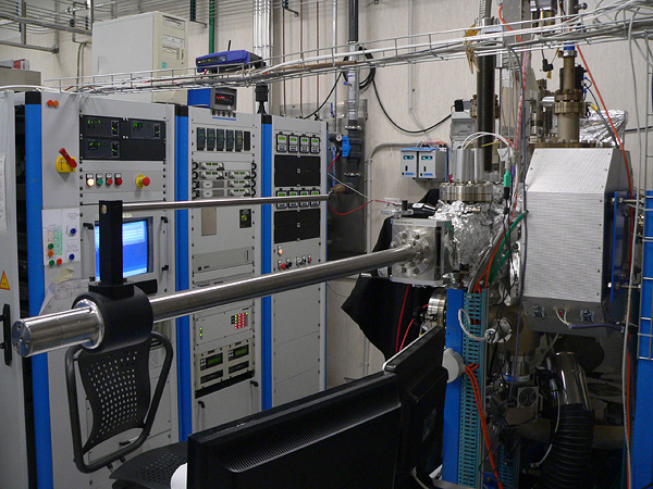
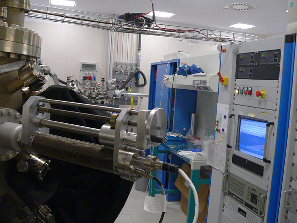
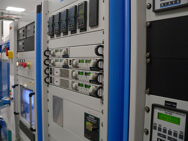
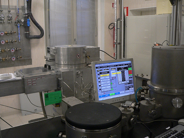
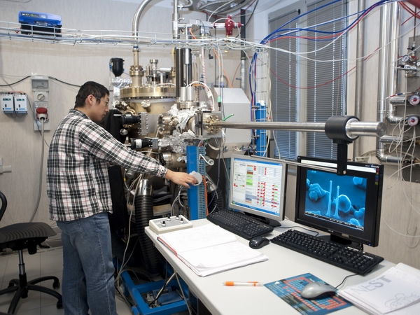
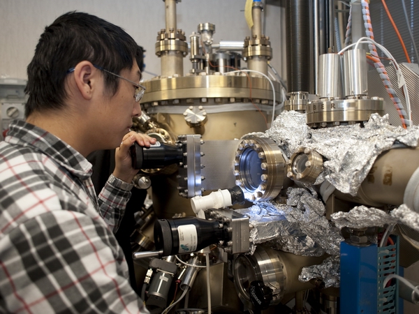
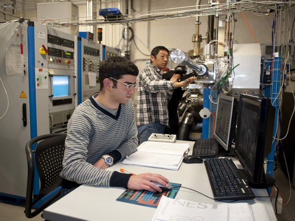
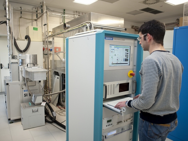
CBE, Plasma Etching and Deposition
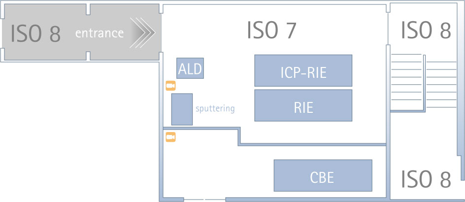
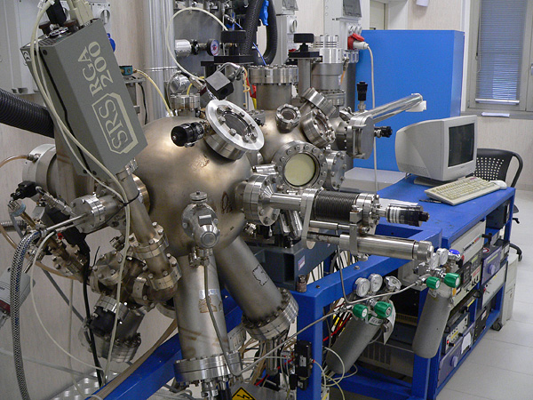
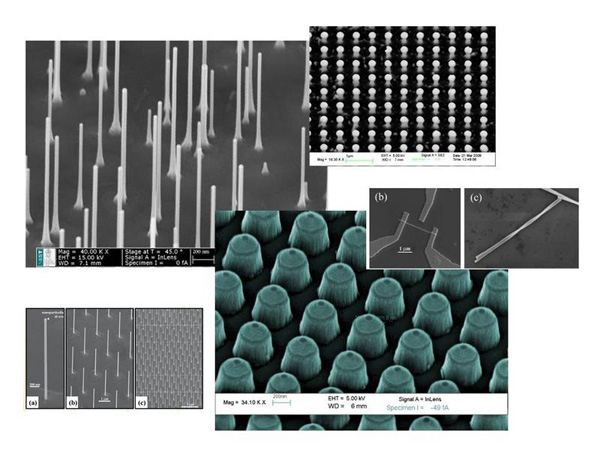
- Chemical Beam Epitaxy for semiconductor nanowire growth;
- Reactive Ion Etching (RIE) system based on CH4/H2 chemistry;
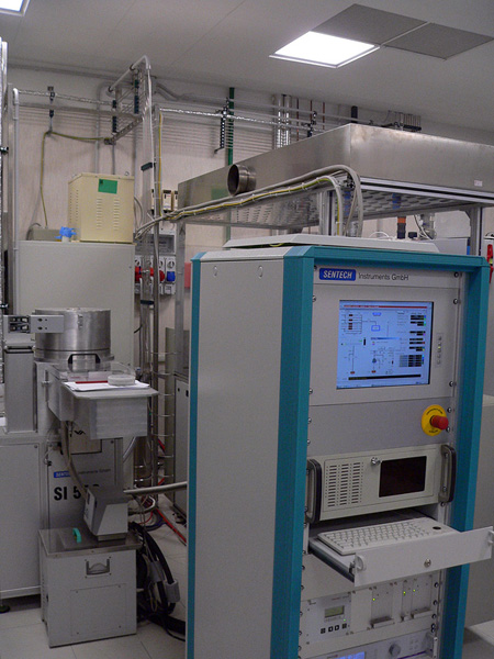
- PECVD system for SiO2 growth;
- RIE-ICP system based on Cl, BCl3 chemistry;
- DC - Sputtering system for Nb and NbN film deposition, Ar sputtering, Sm desorption;
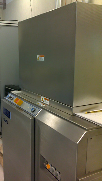
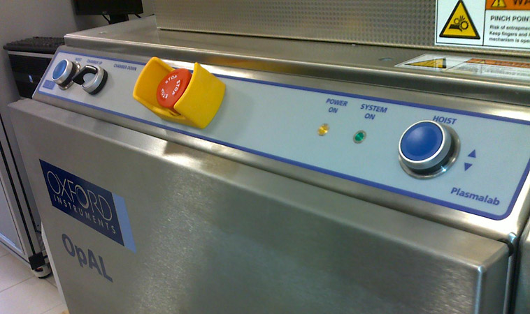
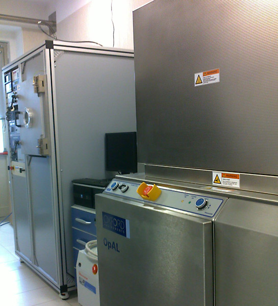
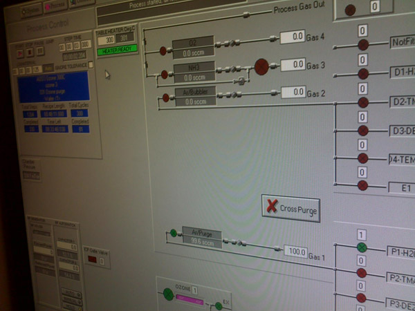
- Atomic Layer Deposition (ALD): "Opal", thermal and plasma system by Oxford Instruments;
© 2009 NEST · Scuola Normale Superiore di Pisa |
W3C quality assurance: xhtml 1.0 strict